- 您现在的位置:买卖IC网 > Sheet目录17360 > IRDC3863 (International Rectifier)BOARD EVAL SUPIRBUCK IR3863
IR3863MPBF
CIRCUIT DESCRIPTION
OVER TEMPERATURE PROTECTION
When the IR3863 exceeds its over temperature
threshold, the MOSFET gates are tri-state and
PGOOD is pulled low. Switching resumes once
temperature drops below the over temperature
hysteresis level.
GATE DRIVE LOGIC
The gate drive logic features adaptive dead
time, diode emulation, and a minimum lower
gate interval.
An adaptive dead time prevents the
simultaneous conduction of the upper and lower
MOSFETs. The lower gate voltage must be
below approximately 1V after PWM goes HIGH
before the upper MOSFET can be gated on.
Also, the differential voltage between the upper
gate and PHASE must be below approximately
1V after PWM goes LOW before the lower
MOSFET can be gated on.
The upper MOSFET is gated on after the
adaptive delay for PWM = HIGH and the lower
MOSFET is gated on after the adaptive delay
for PWM = LOW.
When FCCM = LOW, the lower MOSFET is
driven ‘off’ when the ZCROSS signal indicates
that the inductor current is about to reverse
direction. The ZCROSS comparator monitors
the PHASE voltage to determine when to turn
off the lower MOSFET. The lower MOSFET
stays ‘off’ until the next PWM falling edge.
When the lower peak of the inductor current is
above zero, IR3863 operates in continuous
conduction mode. The continuous conduction
mode can also be selected for all load current
levels by pulling FCCM to HIGH.
Whenever the upper MOSFET is turned ‘off’, it
stays ‘off’ for the Min Off Time denoted in the
Electrical Specifications . This minimum
duration allows time to recharge the bootstrap
capacitor and allows the over current monitor
to sample the PHASE voltage.
COMPONENT SELECTION
Selection of components for the converter is an
iterative process which involves meeting the
One can use equation 5 to find the required
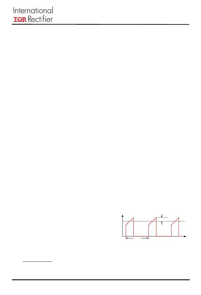
inductance. Δ I is defined as shown in Figure 24.
specifications
and
tradeoffs
between
The main advantage of small inductance is
performance and cost. The following sections
will guide one through the process.
Inductor Selection
Inductor selection involves meeting the steady
state output ripple requirement, minimizing the
increased inductor current slew rate during a
load transient, which leads to a smaller output
capacitance requirement as discussed in the
Output Capacitor Selection section. The draw
back of using smaller inductances is increased
switching power loss in the upper MOSFET,
switching loss of the upper MOSFET, meeting
which
reduces
the
system
efficiency
and
transient
response
specifications
and
increases the thermal dissipation.
minimizing the output capacitance. The output
voltage includes a DC voltage and a small AC
ripple component due to the low pass filter
which has incomplete attenuation of the
switching harmonics. Neglecting the inductance
Input Current
I OUT
Δ I
in
series
with
the
output
capacitor,
the
magnitude
of
the
AC
voltage
ripple
is
determined by the total inductor ripple current
flowing through the total equivalent series
resistance (ESR) of the output capacitor bank.
T S
Figure 24. Typical Input Current Waveform
ΔI ?
T ON ? ? V IN ? V OUT ?
2 ? L
(5)
8/8/2012 Rev3.2
13
发布紧急采购,3分钟左右您将得到回复。
相关PDF资料
IRDC3476
BOARD EVAL SUPIRBUCK IR3476
RO-243.3S/H
CONV DC/DC 1W 24VIN 3.3VOUT
RO-2424S/H
CONV DC/DC 1W 24VIN 24VOUT
MIC2545A-1BTS
IC SW CURR LIMIT HI SIDE 14TSSOP
MIC2545A-1BN
IC SW CURR LIMIT HI SIDE 8-DIP
RO-2412S/H
CONV DC/DC 1W 24VIN 12VOUT
MV036F360M003-CB
VTM CURRENT MULTIPLIER EVAL BOAR
BY255GP-E3/73
DIODE 3A 1300V DO-201AD
相关代理商/技术参数
IRDC3865
功能描述:电源管理IC开发工具 9999V 999A POL IC RoHS:否 制造商:Maxim Integrated 产品:Evaluation Kits 类型:Battery Management 工具用于评估:MAX17710GB 输入电压: 输出电压:1.8 V
IRDC3870
功能描述:电源管理IC开发工具 USER GUIDE FOR IR3870 EVAL BRD RoHS:否 制造商:Maxim Integrated 产品:Evaluation Kits 类型:Battery Management 工具用于评估:MAX17710GB 输入电压: 输出电压:1.8 V
IRDC3871
功能描述:电源管理IC开发工具 USER GUIDE FOR IR3871 EVAL BRD RoHS:否 制造商:Maxim Integrated 产品:Evaluation Kits 类型:Battery Management 工具用于评估:MAX17710GB 输入电压: 输出电压:1.8 V
IRDC3876
制造商:International Rectifier 功能描述:9999V 999.000A POL IC - Rail/Tube 制造商:International Rectifier 功能描述:BOARD EVAL FOR IR3876
IRDC3894
功能描述:电源管理IC开发工具 Design Kit Featuring IR3894M
RoHS:否 制造商:Maxim Integrated 产品:Evaluation Kits 类型:Battery Management 工具用于评估:MAX17710GB 输入电压: 输出电压:1.8 V
IRDC3895
功能描述:电源管理IC开发工具 Design Kit Featuring IR3895M
RoHS:否 制造商:Maxim Integrated 产品:Evaluation Kits 类型:Battery Management 工具用于评估:MAX17710GB 输入电压: 输出电压:1.8 V
IRDC3897
功能描述:电源管理IC开发工具 Design Kit POL IC
RoHS:否 制造商:Maxim Integrated 产品:Evaluation Kits 类型:Battery Management 工具用于评估:MAX17710GB 输入电压: 输出电压:1.8 V
IRDC3897-P1V2
制造商:IRF 制造商全称:International Rectifier 功能描述:USER GUIDE FOR IR3897 EVALUATION BOARD
